At last Wednesday's media event, Apple introduced two new processors - the A10 Fusion for iPhone 7 and 7 Plus and the S2 for Apple Watch Series 2. Although Apple only briefly covered the S2 during the presentation, it did spend a good deal of time talking about A10 Fusion. The 'Fusion' suffix refers to the heterogeneous architecture that the A10 features, which has two high-power, high-throughput cores and two much smaller cores that are more power efficient.
Apple also introduced another very important piece of standalone silicon in its new AirPods, dubbed the W1 chip. In total, this represents a great deal of engineering work done by Apple over the last year, and the A10 is the most significant to Apple's system-on-a-chip (SoC) line since the company's transition to 64-bit.
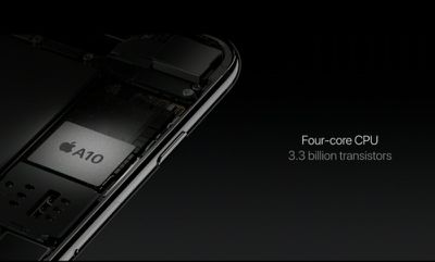
Apple unveiled the biggest technical changes featured in the A10 at the very beginning, boasting a four-core CPU with 3.3 billion transistors. While Apple never disclosed a transistor count for the A9, it very likely fell somewhere in the middle between the 2 billion count on the A8 and the 3.3 billion of the new A10. A transistor count well under 3 billion seems probable for the A9; otherwise it would have been worth boasting about on its own.
The 3.3 billion number for the A10 is well over 50 percent larger than the A8, and the large jump is likely mostly thanks to the addition of two new, albeit small, CPU cores along with a greatly enhanced image signal processor (ISP). Apple also disclosed that the GPU remains a six-cluster design, while benchmarks suggest that the L1 and L2 cache sizes remain unchanged.
Given that the process node is not expected to be different than the A9 fabricated on TSMC's 16nm FinFET process, it is very likely we'll be looking at a larger die size compared to its predecessor. However, it is also likely Apple was able to optimize placement and sizing on what is now a more mature process, without the added complexity of producing a twin design on Samsung's competing 14nm FinFET process.
The leaked logic board shots also suggest a larger device package than the Apple A9, although it is unclear if the new InFO packaging processor has any influence on device package footprint.
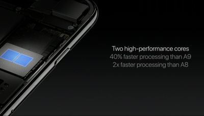
Apple also revealed that A10's peak performance could be up to 40 percent greater than the A9 featured in the previous generation. The 2.33 GHz core speed showing up in benchmarks is roughly 25 percent faster than the 1.85 GHz seen in the A9, meaning Apple has found another 25 percent peak improvement through architecture enhancements.
A 25 percent clock speed increase is significant given that the process node likely did not change, meaning the increase was likely enabled by the better thermal performance of InFO packaging. It is also likely only possible because of Apple's heterogeneous architecture which now features a pair of high-speed cores along with a pair of low-speed, power conscious cores.
Apple's clock speed increase is probably more than just turning up the dial on voltage to make the cores run faster. By introducing the pair of low-speed cores, Apple opened up a whole new spectrum of dynamic voltage and frequency scaling (DVFS) options for completely disabling cores or their sub-parts. Apple designed its own performance controller to manage workloads between the cores, and we know from some industry sources that Apple does cache-sharing so that the caches don't have to constantly read each others' contents to be ready for a switch lest they face a delay in getting current data when they switch on.
This concept may sound familiar because ARM introduced it all the way back in 2011 with the Cortex-A15 "Eagle" design in 2012 with the "big.LITTLE" moniker. ARM's big.LITTLE scheme also features a performance controller and cache coherency mechanisms, but it had to be designed with Linux OS performance management in mind, whereas Apple can retool iOS as needed for any software interfaces to the performance controller. As time goes on, we may learn more about which caches are shared versus which are updated with some coherency mechanism.
The boost to 2.33 GHz clock speeds brings Apple much closer to the clock speeds of competitors from SoC makers such as Qualcomm and Samsung, and Apple may also have made some transistor changes to reach those speeds. By increasing voltage, and choosing transistors with higher static leakage (unavoidable waste power), Apple can get to these higher clock speeds. Apple's chip team can also make architectural designs that have a higher power footprint in general, whether it be at a higher transistor count, more management power overhead, or more switching activity through a different logic implementation.
The takeaway is that making these sacrifices is now okay because they are more equipped to deal with the thermal implications, and they don't have to deal with the static power draw of all of these changes when the circuit is not in active use because they can simply turn it off and switch to the low power core.
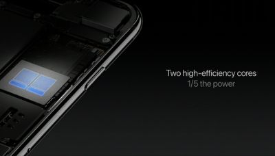
Apple's two small cores in the A10 have drawn just as much interest as their larger cousins, with a lot of speculation centered on whether they too are an Apple custom design, or if they are a variant of a stock low-power core from ARM, such as the Cortex-A53. After so many years of full custom designs, it is fair to ask why Apple would opt for an off-the-shelf solution for its low power CPU, but there is certainly still precedent for it.
By all indications, the first-generation Apple Watch features a Cortex-A7 CPU design. The Apple Watch comparison is interesting because Series 2 was merely increased to a dual-core design up to 50 percent faster than the original. The same question of custom vs. stock design is relevant here, and it is possible that the dual-core CPU in S2 is the same dual-core featured as the low-power option in A10.
The main question centered around this architecture shift is why now would be the appropriate time for Apple to do a heterogeneous architecture. One possibility is that Apple's main core designs had been optimized so much that there were few gains to be had, and those gains would have been with serious diminishing returns. Ratcheting up the clock speed is an easy way to get more performance, but the thermal and power costs associated with that may have been the driving force for the split.
Die size is not unlimited either, and as long as there were gains to be had by making the CPUs bigger, Apple may have opted to go that route. The enhanced functions of the ISP may have also been a good reason to raise the L3 SRAM cache from 4 MB to 8 MB, which does have some impact on the die size as well. Going forward, it's important to remember that CPU clock speed won't be unlimited either, as high-end desktop CPUs have been stuck between 3 GHz and 4 GHz for the past decade, for example.
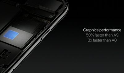
Apple finished up its technical disclosure by talking about the graphics power of the A10. Fortunately, Phil Schiller mentioned it was a six-cluster design, so we know it matches the cluster count on the A9. Apple's performance claims also suggested that the A10 GPU can be up to 50 percent faster than the A9's GPU while consuming only 2/3 the power.
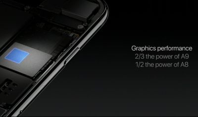
We also know Apple used the same process node for the A10 as on the A9. Since the announcement of the 7XT series of GPUs from Imagination Technologies that was featured in the A9, there has only been one new type of high-performance GPU announced from ImgTec, and it was simply to add computer vision and compute performance enhancements to the existing 7XT line.
The power reduction alone rules out that Apple increased clock speeds to make these performance claims, so we are likely looking at some significant changes that feature an unannounced GPU, an Apple-designed GPU, or some other major architectural shift that we don't know about. It is possible Apple could claim some gains through enhancements in metal, but up to 50 percent improvement in speeds seems a rather high claim for that.
Apple's performance boost claims have historically tended to actually show in benchmarks, so this will be an area of particular interest when the GPU gets fully benchmarked and pictured under a microscope.
The introduction of Apple's AirPods was also an important moment because they feature Apple's new W1 wireless connectivity chip. In the announcement, Phil Schiller put special emphasis on it being Apple's first wireless chip, suggesting that there are more to come. We have been waiting several years since Apple first hired several RF engineers from Broadcom, and this small Bluetooth chip could be a stepping stone to Apple providing its own RF components such as the Wi-Fi chip or even the cellular baseband modem in future devices.
This is a very tough sector to get into and be a competitor in the general marketplace, however, as seen with Intel's own LTE offerings likely featured in the new iPhone, for example. Rather than being built from the ground up, those chips are the product of Intel's acquisition of Infineon and manufactured on a TSMC process rather than Intel's own. The potential gains for custom wireless chips are also less clear than with fully custom CPU solutions seen in SoCs, so this does not necessarily mean Apple's ambitions stretch that far.
We're likely to find out much more in the coming weeks as the teardowns begin, exhaustive benchmarks are run, and the more advanced analyses from firms such as Chipworks begin to trickle out. From there, we'll have a better picture of the specific methods and techniques Apple has used to increase chip performance and potentially have a better idea of what's coming next.




Top Rated Comments
They keep saying, iPhone has the power of an Xbox360, or even better now.
So where are all the XBox 360 quality games for the iPhones?
Plug in a big screen, and play Xbox 360 or better titles from your phone.
But what do the App Devs give us?
Crossy Road, or some sad mario side scroller, or some other pointless game that are hardly above the old flash based web page games.
Why are people not making PROPER decent full games for these devices?
It's such a waste. :(
I'm amazed they got 25% extra from one generation, in a non-S series model. Historically the jump between shells (3GS to 4, 5S to 6), hasn't offered anywhere close to this sort of improvement.